


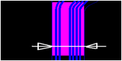
In the FPC (flexible printed circuit), we will provide a wide range of products, FPC flexible circuit switch series GOOYU offers a variety of space choice, and contains a variety of functions, can meet various application and use of the space of all market demand, and strong waterproof performance, and good impedance, very suitable for compact packaging applications.
The Gooyu FPC connector provides push and flip drives that have been pre equipped with lids to secure the connections between the FPC and connector terminals. GOOYU is developing smaller, more compact models to meet the needs of electronic equipment manufacturers for leaner sizes.


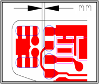
The flexible PCB board is designed to meet the requirements of a high performance internal connection, using a variety
of combinations of materials to achieve the product's use requirements
Project
Category
Conventional ability
General ability
Plate size
Min (Pcs Size)
5 ×5 mm
Max (Pcs Size)
238*440mm
Max (Pnl Size)
250*450mm
Substrate thickness
Min
0.05 mm
Max
2.0 mm
Thickness tolerance of finished products
Plate thickness < 0.5mm & nbsp; (including FR4 reinforcement, steel sheet reinforcement)
±0.050 mm
0.5mm < plate thickness & nbsp; (FR4 reinforcement, steel sheet reinforcement)
±10%
0.30mm < plate thickness & nbsp;(PI Reinforcement)
±0.020 mm
0.30mm ≤ plate thickness <0.5mm & nbsp;(PI Reinforcement)
±0.030 mm
0.5mm < plate thickness & nbsp; (PI Reinforcement)
±10%
Bottom copper thickness
Min
1/3OZ
Max
2OZ
Copper Thickness of PTH Hole Wall
N/A
1-35μm
Copper Thickness Tolerance of Controllable Hole Wall
N/A
±3 μm
TP value of copper plating
N/A
180-200%
Ratio of Longitudinal to Transverse Filling Capacity of Blind Hole (Aperture: Depth of Hole)
N/A
1.5-2.5
Blind hole filling capacity (aperture size)
N/A
50-150μm
Thickness of FPC Insulation Layer
Min
8 μm(PI thickness)
Max
90 μm(PI厚50μm,AD 厚40μm)
Glue overflow of covering film
BGA Special Covering Film
<0.1 mm
Common Covering Film
<0.15 mm
peel strength
base material
0.70 kgf/cm
Covering film
0.65 kgf/cm
PI/FR4 reinforcement
1.0kgf/cm
Reinforcement of steel sheet/aluminium sheet
1.0 kgf/cm
Single line impedance tolerance
N/A
±10%
Differential impedance tolerance
N/A
±10%
Minimum Linewidth Line Spacing (Double Panel)
Surface copper thickness:8-14μm
45/45 um
Surface copper thickness:15-20μm
50/50 um
Surface copper thickness:21-30μm
55/55 um
Surface copper thickness:31-40μm
75/75 um
Surface copper thickness:≥40μm
80/80 um
Line width tolerance
Linewidth ≤0.070mm
-0.02mm
0.07mm<line width≤0.15mm
±20%
Linewidth>0.10mm
±10%
Solder resist
Minimum Width/Spacing of Screen Printed Characters
N/A
5/6mil
Silk screen printing
Green oil thickness range
Line thickness
10~30 μm
Relevant
Dimensional tolerance from edge of white oil line to edge of plate
N/A
±0.25 mm
Width tolerance of white oil line
Smooth place
±0.10 mm
Concave convex place
±0.20 mm
Aperture correlation
Minimum borehole diameter
Mechanical drilling
0.100 mm
Minimum punching aperture
N/A
0.50 mm
Perform aperture tolerance
Plated through hole
±0.050 mm
Non plated through hole
±0.025 mm
SLOT Aperture Tolerance
Plated through hole
L/W>2:1:
Minimum aperture: 0.60 mm
Width:±0.050mm Length :±0.125mm
Non plated through hole
L/W>2:1:
Minimum aperture: 0.60 mm
Width:±0.025mm Length :±0.1mm
Shape and size
Minimum width of shape
N/A
1.0 mm
Minimum opening size of covering film
Punching Dimensions Using Dies
0.5mm
Using borehole size
0.35mm
Minimum Clearance of NPTH Hole in Steel Die Punching
N/A
0.50 mm
Dimensional tolerance from hole center to hole center
Drilling hole drilling
±0.075 mm
Punching die
±0.075mm
Precision steel die punching
±0.050 mm
Circuit, PAD, Hole and Finger Center
N/A
±0.10 mm
Size tolerance to edge of plate
±0.075 mm
PITCH (span)
≤100mm
±0.05 mm
100mm<PITCH≤200mm
±0.07 mm
>200mm
±5%%
Center distance tolerance of adjacent fingers
N/A
±0.025 mm
Contour tolerance
Steel mould
±0.1mm
Precision steel mold
±0.05mm
All kinds of counterpoint ability
Alignment accuracy of covering film and reinforcement
Manual counterpoint
±0.20 mm
Alignment of jig
±0.15 mm
Automatic alignment (CCD equipment)
±0.10 mm
Alignment accuracy of electromagnetic film and glue
Manual counterpoint
±0.20 mm
Alignment of jig
±0.15 mm
Graphic alignment accuracy
Same layer
±0.05mm
Upper and lower levels
±0.05mm
Anti-welding alignment accuracy
N/A
±0.050 mm
Alignment Accuracy of Silk Printed Texts
N/A
±0.30 mm
surface treatment
Plating Ni/Au
Nickel thickness
1~ 8 μm
Thickness Tolerance of Nickel Layer
±2μm
Jin Hou
0.03 ~ 0.15 μm
Minimum spacing (golden finger or Pad)
35um
Nickel deposit
Nickel thickness
1 ~ 6 μm
Thickness Tolerance of Nickel Layer
±1μm
Jin Hou
0.03 ~ 0.075 μm
Minimum spacing (golden finger or Pad)
40um
OSP
OSP层厚
0.15~0.5μm
Expansion and contraction control capability
Controlling Tolerance of Controlling Length for Expansion and Shrinkage
Control tolerance
Control length
Cpk≥1.33
Cpk≥1.0
±0.030
≤30
≤40
±0.040
≤40
≤50
±0.050
≤50
≤70
±0.075
≤75
≤100
±0.100
≤100
≤135
±0.125
≤125
≤165
±0.150
≤150
≤200
Project
Conventional ability
Graphic
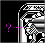
Relevant Capacity of Line Design
Minimum Spacing between PAD and Circuit, PAD and PAD (Covering Film Process)
0.25 mm
Minimum Spacing between PAD and Circuit, PAD and PAD (Ink Process)
0.15 mm
Minimum Spacing between Parts PAD and Large Copper Skin
0.15 mm

Minimum gap (etching line) between the edge of the PAD through the hole or the line to the copper
0.03mm
Minimum Spacing between PTH Hole and PAD Edge of PTH Hole (Etching Circuit)
0.03mm

Minimum gap between AD with weld-proof window and circuit
0.13 mm
Relevant Ability of Weld Resistance Design
Minimum Width of Weld Resistance Bridge
Green oil: 0.10mm black oil: 0.15mm

Ability to design other tools
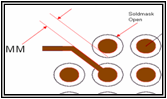
Minimum Spacing of Window Opening with Different Covering Films
0.3 mm
Minimum width of PI reinforcement
2.0 mm
Minimum Width of FR4 Reinforcement
3.0 mm
Minimum Width of Adhesive Paper/Steel Sheet Reinforcement
2.0 mm
Minimum spacing between reinforcement and electromagnetic film
0.25 mm

Minimum Spacing between NPTH Hole and Large Copper Skin
0.1 mm
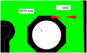
The Minimum Distance Between NPTH Hole and Circuit, NPTH Hole and PAD, NPTH Hole and Board Edge
0.3 mm

Minimum spacing between NPTH holes and NPTH holes
0.5 mm

Minimum distance from element to plate edge
0.3 mm
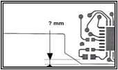
Minimum distance from line to board edge
0.15 mm
Minimum Distance from PAD Edge of PTH Hole to Plate Edge
0.3 mm
Product
下载中心


